IIT Guwahati, Columbia University collaborate to develop optical driving process for nanopatterns
Alivia Mukherjee | May 23, 2024 | 04:53 PM IST | 2 mins read
In partnership with Columbia University, IIT Guwahati researchers devised a new approach that uses "optical driving" to produce vibrations in materials at their resonance frequency, leading to accurate cleavage along clean lines.
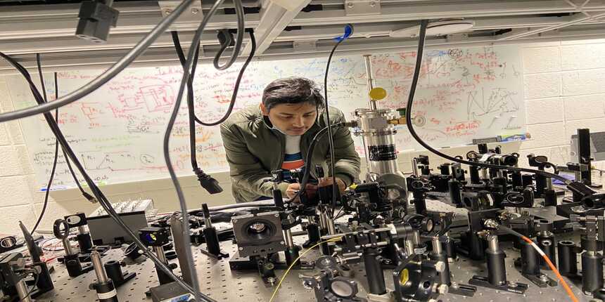
NEW DELHI: Scientists at the Indian Institute of Technology (IIT) Guwahati and Columbia University in the United States have devised a nanopatterning method that makes use of a simple tabletop IR laser. Rishi Maiti, assistant professor in the Department of Physics at IIT Guwahati and a former post-doctoral scientist in Alexander Gaeta's quantum and nonlinear photonics group, has published the research findings in the journal Science Advances.
Nanopatterning is the process of creating patterns on materials at the nanometer scale, which is significantly smaller than the width of a single human hair by a factor of one hundred thousand. This method allows for the production of nano-sized optical components and polariton cavities, essential for the development of devices like sophisticated light sensors, solar panels, lasers, and LEDs.
Optical driving as an accessible alternative
Traditional techniques for nanoscale patterning typically demand specialized equipment and facilities, including clean rooms for electron beam lithography machines, or methods involving intense local heating and plasma from direct writing. In pursuit of a more accessible and cost-effective solution, a multi-institutional team has embraced a less demanding process known as "optical driving," harnessing the resonance frequency principle within materials.
Unzipping method
Using a method called "unzipping," scientists fragmented hexagonal boron nitride with an infrared laser, producing atomically precise lines spanning a few nanometers in width across the sample. The laser wavelengths at 7.3 micrometers enabled precise lattice cleavage, leading to the creation of manageable nanostructures.
The scientists utilized the "unzipping" technique to create two parallel lines, generating a nano-scale cavity capable of confining phonon-polaritons, distinct quasi-particles originating from the interplay between light and vibrations. These confined particles possess the ability to focus light into sub-nanometer regions, offering potential advantages for extremely sensitive mid-infrared sensing and spectroscopy applications.
Rishi Maiti, assistant professor, department of Physics, IIT Guwahati and co-author of this work, said, "This novel nano-patterning technique using optically induced strain opens doors to a myriad of possibilities in nanoscience and technology. Its simplicity and effectiveness mark a significant advancement in the field, with far-reaching implications across various industries.”
Disclaimer: This content was distributed by IIT Guwahati and published as part of Careers360’s marketing initiative.
Follow us for the latest education news on colleges and universities, admission, courses, exams, research, education policies, study abroad and more..
To get in touch, write to us at news@careers360.com.